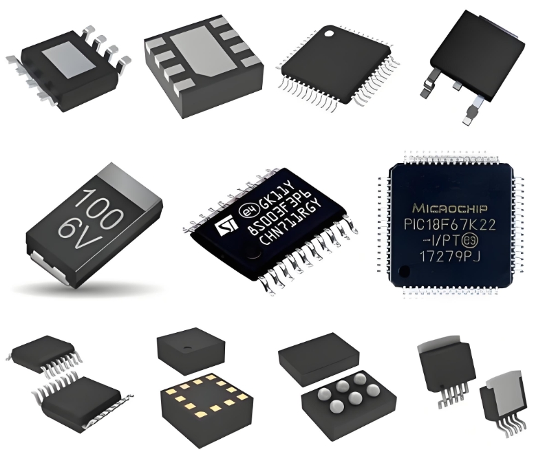
Lattice GAL18V10B-20LP: Architecture, Key Features, and System Design Applications
The Lattice GAL18V10B-20LP stands as a classic and highly influential device in the history of programmable logic. As a 20-pin, low-power (LP) Generic Array Logic (GAL) device, it provided a powerful and flexible solution for a wide range of digital logic applications, succeeding the earlier PAL (Programmable Array Logic) architectures. Its enduring legacy is built on a robust architecture, user-reprogrammability, and system-level reliability.
Architecture: A Look Inside
The architecture of the GAL18V10B-20LP is elegantly simple yet powerful. It is based on a programmable AND array feeding into a fixed OR array. This structure allows designers to create custom sum-of-products logic functions. The "18V10" designation breaks down as follows: the '18' refers to the number of inputs, and the '10' refers to the number of outputs.
The heart of its flexibility lies in its Output Logic Macro Cells (OLMCs). Each of the ten outputs is controlled by a dedicated OLMC, which can be configured by the user to operate in various modes:
Combinatorial Mode: The output is solely a function of the AND-OR array.
Registered Mode: The output is stored in a D-type flip-flop on the rising edge of the clock signal, enabling the design of sequential logic circuits like counters and state machines.
Complex Mode: Allows for configurations where an output pin can also serve as an input, providing additional flexibility for pin-constrained designs.
This configurability of the OLMCs is what truly set the GAL device apart from its one-time programmable (OTP) PAL predecessors.
Key Features and Advantages
The GAL18V10B-20LP introduced several key features that cemented its popularity among engineers.

Electrically Erasable (E²) CMOS Technology: This is its most significant advantage. Unlike OTP PALs, the GAL device can be reprogrammed thousands of times. This drastically accelerated prototyping, design debugging, and firmware updates, reducing both development time and cost.
Low Power Consumption: Fabricated in CMOS technology, the device operates with very low static and dynamic power, making it suitable for portable and battery-operated applications.
High Speed: With a maximum propagation delay of 20 ns (as denoted by the -20 in its part number), it was capable of operating at high clock frequencies for its era, satisfying the requirements of many performance-critical applications.
100% Testability & High Reliability: The architecture supports full functional testability. Furthermore, its integrated security fuse prevents unauthorized copying of the programmed logic pattern, protecting intellectual property.
System Design Applications
The flexibility of the GAL18V10B-20LP made it a ubiquitous "glue logic" component in countless digital systems throughout the 1990s and early 2000s. Its primary role was to integrate multiple standard TTL (Transistor-Transistor Logic) chips into a single, compact device, reducing board space, component count, and system power consumption.
Typical system design applications included:
Address Decoding: Generating chip select signals for microprocessors (e.g., 8051, Z80, 68000) in memory-mapped systems.
State Machine Control: Implementing finite state machines (FSMs) for controlling system processes, such as timing sequences and interface protocols.
Bus Interface Logic: Acting as an interface between buses with different protocols or timing requirements.
Code Conversion and Data Gating: Performing simple data manipulation, multiplexing, and signal conditioning tasks.
ICGOODFIND: The Lattice GAL18V10B-20LP was more than just a chip; it was a foundational technology that democratized digital logic design. Its reprogrammable nature, flexible OLMC structure, and CMOS efficiency empowered a generation of engineers to innovate rapidly, consolidating complex logic and enabling the creation of more sophisticated and reliable electronic systems. It served as a critical bridge between simple fixed-function logic and the high-density FPGAs and CPLDs that followed.
Keywords: Programmable Logic Device, Output Logic Macro Cell (OLMC), Electrically Erasable (E²) CMOS, Glue Logic, Sum-of-Products
